A spring network simulation in three dimensions for designing optimal crack pattern template to fabricate transparent conducting electrodes
S. Sadhukhan, A. Kumar, G. U. Kulkarni, S. Tarafdar, T. Dutta
Bull. Mater. Sci 42(5), 2019
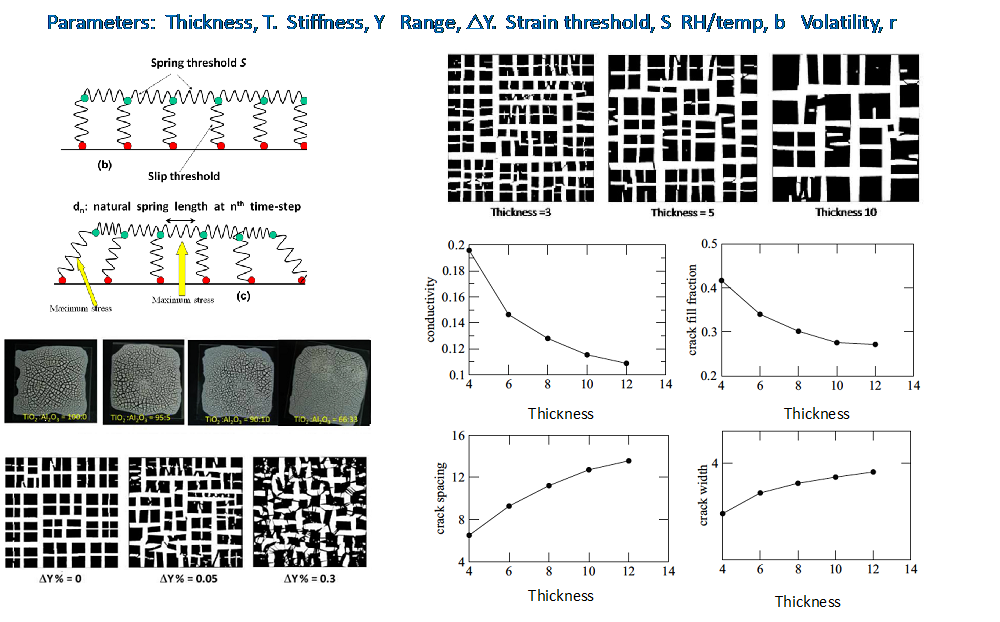
Desiccating cracks often form a well-connected network structure in the colloidal film due to stress arising from desiccating process. Interestingly, desiccating crack patterns can be used as a suitable lithography template for fabricating metal network based transparent conducting electrodes (TCE) for optoelectronic applications. An optimum crack pattern is desired for realizing optimum metal wire networks with high transmittance, conductance and effective charge collection properties. In this work, we simulate crack pattern in desiccating colloidal films in three dimensions using a spring network model. A colloidal film is modeled as an array of springs, with individual spring representing bond between neighboring colloidal particles; the desiccation process leads to shrinkage of these springs and eventually breaking of few of them leading to the formation of the crack pattern. We look for the optimal combination of system parameters, such as film thickness, material stiffness and polydispersity, which can produce the best template for producing a conducting network on transparent surfaces. Thus, the present study will be useful in the direction of crack physics, electrical percolation and engineering of crack patterns for efficient TCE applications.
Posted by A. Kumar.