Defining switching efficiency of multi-level resistive memory with PdO as example
K. D. M. Rao, A. A. Sagade, R. John, T. Pradeep and G. U. Kulkarni
Adv. Elec. Mater., 2, 1500286 (2016)

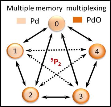
Resistive random access memory (RRAM) is the most promising candidate for next generation nonvolatile memory. In this article, resistive switching in PdO thin film is investigated. The fabricated in-plane devices showed voltage pulse induced multilevel resistive switching (MRS) with as many as five states under ambient conditions with high degrees of retention and endurance. The I–Vcharacteristics of the different memory states are linear and only a small reading voltage (≈10 mV) is necessary. Raman mapping of PdO (B1g mode, 650 cm–1) and temperature-dependent electrical transport measurements provide an insight into possible redox mechanism involving PdO/Pd particles. For the first time, the switching efficiency of a MRS device is uniquely defined in terms of a parameter called “multiplex number (M),” which is the sum of the total number of memory states and the ratio between the number of switching events observed in a device and the total number of possible switching events. The present PdO MRS device exhibits the highest M value compared to the values evaluated from the literature examples. Such high performance MRS in PdO devices makes them potential candidates for RRAM and neuromorphic circuit applications.
Posted by Dr. K. D. M. Rao
