
Through the years, the lens has always amazed me due to its simple design and versatility of usage. I used to wonder why my paati’s (grandma) spectacles were so thick and heavy… And the camera carried by our family photographer (in the ‘pre-smartphone era’) so bulky… Since then, there has been a lot of development in making the lenses, especially in eyewear and professional cameras, more compact. Still, it has not reached a stage where one can wear the spectacles comfortably without leaving a mark on the nose or carry a bulky camera without being awkward! Can we make the lens thinner and flatter to make spectacles and cameras more ergonomic? The question leads to the fascinating journey of a humble lens evolving into the exotic ‘metalens’!
The origin of lens can be traced back to around 700 BCE, when ancient Egyptians and Mesopotamians used polished crystals (eg. ‘Nimrud lens’) to magnify objects. Even the term ‘lens’ comes from the Latin name “lēns”, meaning “lentil” because of the shape! Towards the 13-15th centuries, Europeans started crafting wearable eyeglasses using lenses. The applications went beyond eyewear, and in the 16th century, Robert Hooke invented the microscope, and Galileo and Kepler, the telescope. Fast-forward to the 21st century… lenses are used in a myriad of applications ranging from magnifying glass (the simple optical tool, which many of us would have used to burn papers in our proud science at home experiments during high school days), spectacles, cameras, to high-end microscopes and telescopes.
Modern technological advancements have resulted in sophisticated gadgets/ tools such as smartphones, augmented/virtual reality headsets, micro/nanoscale robots, etc. which demand compact lenses without compromising the imaging quality. As the thickness of the glass lenses reduces, precisely shaping them becomes all the more complex (see Figure 1), resulting in various aberrations, which distort the images. Further, for high-end imaging applications like microscope objectives, several lenses need to be stacked on top of each other to correct the aberrations (see Figure 1), which makes the system bulkier. Another fundamental limitation is that a conventional lens cannot resolve two objects which are closer than ~ 0.5 λ (λ being the operating wavelength), which is known as the ‘Abbe diffraction limit’. To overcome these challenges, what if we could reimagine the lens as a compact flat surface yet provide the necessary curvature to focus the light waves?!…
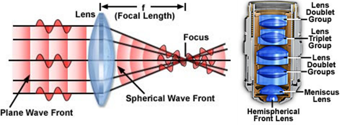
Figure 1: Schematic representation of (left) plane wave front of incident light getting converted to a spherical wavefront by a convex lens, (right) stacked lenses of a high-end microscope objective
A metamaterial – based lens (or) meta lens does precisely the same thing. Metamaterials are artificially structured materials used for controlling / manipulating light, sound, temperature and several more physical properties. The structure is due to the arrangement of sub-wavelength sized objects known as ‘meta-atoms’ or ‘meta-molecules’. In the year 2000, Prof. John Pendry from Imperial College, London proposed the idea of metalens that is capable of resolving objects beyond the diffraction limit. His prediction sparked a plethora of research activities in the field. In 2005, Prof. Xiang’s group at Univ. of California, Berkeley realized such a meta-lens with a 35 nm thin film of silver, exhibiting sub-diffraction limit resolution. In 2016, Prof. Federico Capasso from the Harvard University, USA, pioneered the fabrication of metalens from dielectric metamaterials/or metasurfaces, to achieve reduction in the optical losses and enhancement in efficiency.
To appreciate the advantages of meta lens, let’s look at how a lens actually interacts with light. For any wave, the surface over which its phase is constant is called a wavefront. As the thickness of a conventional lens varies continuously from the mid-point to the periphery, the light wave passing through it experiences a continuous phase shift, leading to a converging wavefront. This results in a focussed image of the object (see Figure 1).
Now let’s see how a metalens works. The meta lens consists of several nano-sized structures(e.g.pillars or discs) fabricated on a flat surface. The material and dimensions of these structures (or nanoantenna) are carefully chosen to provide a phase shift (which varies between 0 and 2π) to the incoming light wave. The structural arrangement is done in such a way that the phase increases sequentially from the middle towards the periphery. The discontinuous phase shifts thus created converge the wavefront of the incoming light wave, resulting in a focussed image
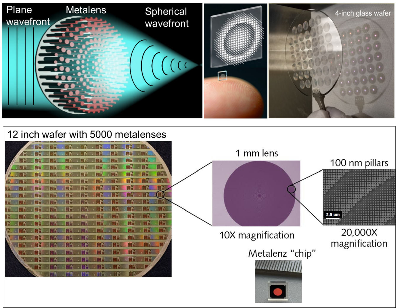
Figure 2:Top panel: (left) Schematic representation of the incident plane wave front getting converted to a spherical wavefront by a metalens, (middle) Artistic representation of single metalens sensor, which is as tiny as a grain of salt.(right) Focussing of light by the all glass metalens demonstrated by Capasso’s group, in which 45 metalenses are fabricated onto a 4 inch dia glass wafer. Bottom panel:Photographs depicting the various components of the 12 inch wafer consisting of metalens chips fabricated with TiO2 nanopillars demonstrated by the startup company ‘Metalenz’.
Thus, we have a metamaterial- based lens, only a few millimetres in diameter and an active layer thickness of few 100 nanometers, and does the job of a conventional lens! (see Figure 2 top panel). The flat surface of the ‘metalens’ naturally removes the spherical aberration, and scales down the possibility of other aberrations (chromatic, astigmatism etc.) by an order of magnitude compared to a conventional 3-dimensional lens. Aberration correction by stacking several lenses becomes much easier in the flat metalens. Further, while imaging any object through a lens, the high spatial frequency evanescent waves, which carry the sub-wavelength information from the object exponentially decay within the ‘near field’ (i.e.less than one wavelength distance) of the lens. But, in a metalens, the resonance phenomena occurring in the nanoantenna amplify the evanescent waves and couple them to the far-field. Thus, the metalens is capable of sub-diffraction limit resolution, i.e., it can resolve two points of an object beyond the ‘Abbe diffraction limit’. All these features essentially mean sharper and clearer images with thinner and lightweight lenses.
In 2019 Prof. Capasso’s group fabricated an array of 45 metalenses of 2 μm height and 1 cm diameter each on a 4 inch glass wafer (see Figure 2 top panel). The success led to a startup company, ‘Metalenz’ (Boston, USA)based from his lab, which is mass-producing metalenses using TiO2 nanopillars for specialized smartphone sensors (see Figure 2 bottom panel).
With continuous improvements being made, e.g., tunable focus and aberration correction from various research groups worldwide, metalenses are proving to be quite promising compared to their curved counterparts. It is only a matter of time…, the metalenses will outperform conventional lenses and lead to a new world of ultrathin flat optics.
Dr. S. Vimala
Research Associate
Dr. Geetha G. Nair’s research group
CeNS, Bengaluru